Probe Needle Materials for Wafer Testing
Wafer Testing (also known as EDS - Electrical Die Sorting) is an elementary step in the production of any semiconductor structure and process technology. More specifically, after the integrated circuits are manufactured and before they are separated from the wafer, all individual electrical contacts are tested for functional defects according to specific electrical test patterns. This integrated circuit test (also known as CP - Circuit Probe) is performed by automated test units and requires a high level of reliability in the interface between the tester and the wafer contact pad. This interface is provided by probe cards and probe needles.
High demands are placed on the probe needles in the probe card. Due to the minimal pitch distances between the individual contact pads, they must be extremely straight and have excellent electrical conductivity. In addition, they must be sufficiently elastic and have good mechanical strength even at high temperatures to be used over many load cycles and touchdowns. The most important metric for probe card efficiency is to reduce the cost per test, the time per test and to increase the number of parallel tests while minimizing contamination (low contact resistance CRes).
Heraeus Solutions for Your Test Requirements
Heraeus offers a wide range of probe pin materials from precipitation hardened PdAgCu alloys to high-strength PtNi alloys. Probe pin materials made by Heraeus can be applied for any probe card type: from cantilever to vertical to MEMS type and advanced probe cards with a consistently high quality standard.
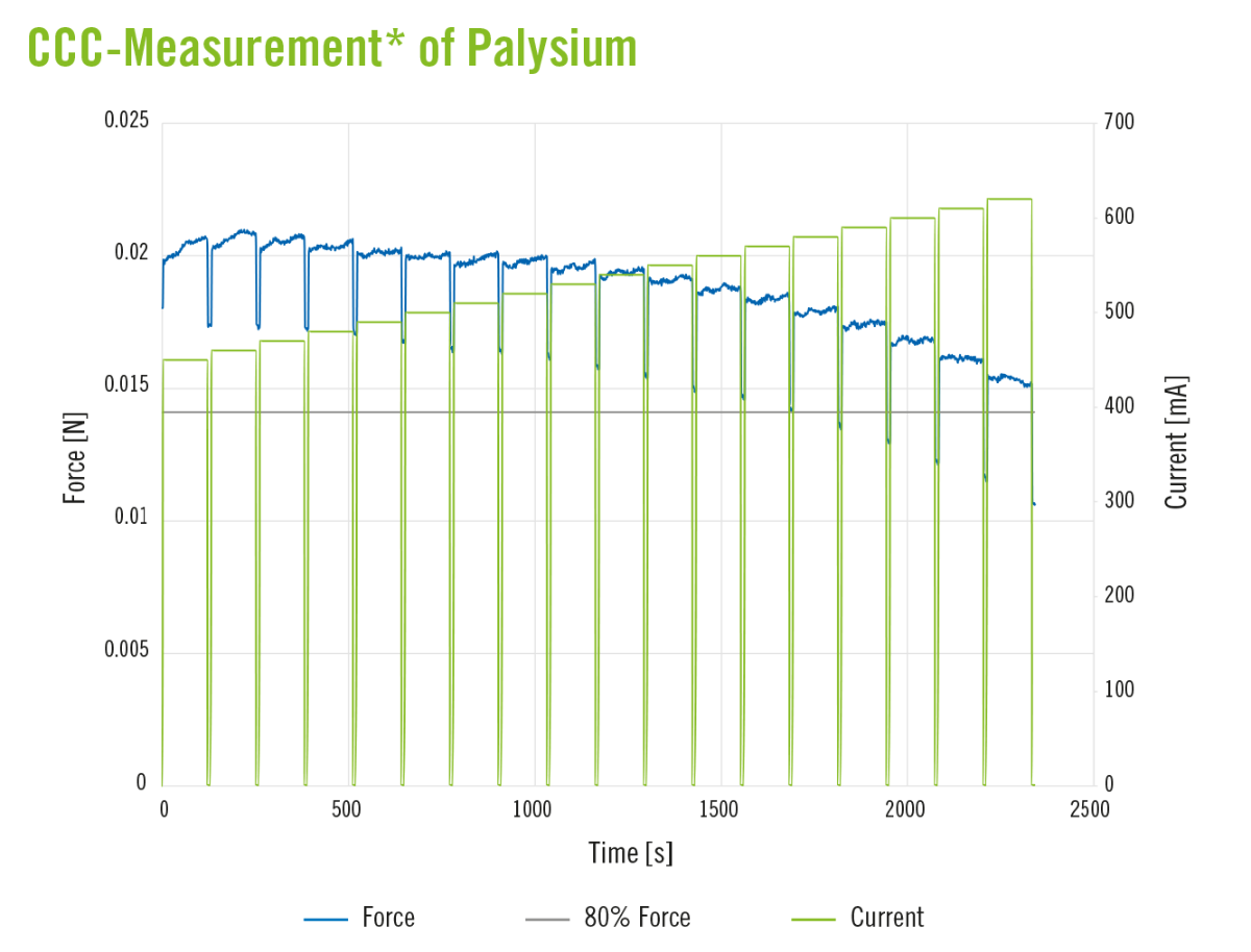
Heraeus has led the way in the production of customized high-performance materials to the semiconductor industry for more than 50 years. In addition to many years of experience, Heraeus is your partner in identifying and processing the optimal material for your application. Furthermore, customers benefit from CCC/MAC testing as well as surface analysis.

Your Benefits
1. We melt the alloy you need
- Material properties can be adapted to your requirements through a combination of different diameters and hardening processes
- Variety of alternative materials to select the perfect match for your application
- Excellent electrical conductivity and mechanical characteristics to achieve longlasting and reliable probe performance
- Extremely dimensionally stable materials demonstrating high strength, elasticity, and thermal resistance for manufacturing very accurate probe needles
2. We customize our products to your needs, from alloying to ultrafine wires
- Supportive advice on choosing and adapting the right material and configuration for your application.
- Consistently high standard of quality & fast delivery times
- Complete precious metal cycle - from purchasing to manufacturing to recycling
3. We innovate materials for your next-gen test equipment
- Unique combination of material expertise, application and manufacturing know-how
- Extensive possibilities for mechanical/electrical testing (CCC/MAC) and surface analysis in Heraeus’ inhouse labs
Palysium
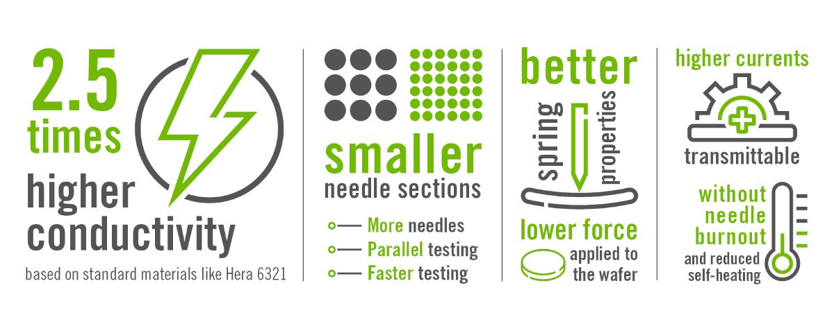
Palysium is a Heraeus alloy developed specifically for semiconductor test applications. Due to its unique superlattice structure, Palysium has very high electrical conductivity (2.5 times higher than the PdAgCu market standard Hera 6321), combined with excellent spring properties and processing capabilities for wire diameters up to 15 μm.

This enables the production of very accurate and smaller needle sections that allow reliable testing of smaller pitch sizes, as significantly more current can be transmitted for the same cross-sectional area. At the same time, the needles can shrink considerably at the same current, which has a positive effect on pitch, needle count and test parallelism.

Specialized Alloys tailored for your Semiconductor Testing Application
From standard materials to new metallurgical solutions of advanced alloys, the development focus is on good spring properties, high conductivity, and high durability, with mechanical properties adjustable to individual requirements.

|
Hera 648 |
Hera 6321 |
Palysium |
Hera 1206 |
Hera 5270 |
|
|---|---|---|---|---|---|
| Main Components [wt%] | Pd35 Ag30 Au10 Pt10 | Pd39 Ag29 | Pd52 Ag11 | Pt Ni31.5 | Rh dot |
| Density [g/cm3] | 11.8 | 10.4 | 10.5 | 15.1 | 12.4 |
| Young’s Modulus [GPa] | 108 | 112 | 120 | 234 | 330 |
| Yield Strength Rp0,2 [MPa] | 1050 - 1350 | 1100 - 1600 | 1250 - 1450 | 1500 - 1900 | 1900 - 2500 |
| UTS [MPa] | 1100 - 1400 | 1200 - 1700 | 1300 - 1500 | 1600 - 2000 | 2100 - 2700 |
| Hardness [HV] | 330 - 400 | 400 - 450 | 400 - 500 | 400 - 490 |
up to 530 |
| Thermal Conductivity [W/mK] | 28 | 66 | 144 | 150 | |
|
Electrical Resistivity [μ0hm*cm] |
35.9 - 33.2 | 21.3 - 12.3 | 7.2 - 6.4 | 41.0 - 33.2 | 5.7 - 5.4 |
| IACS [%] | 4.8 – 5.2 | 8.1 – 14.0 | 24 - 27 | 4.2 – 5.2 | 30 - 32 |
| CCC [mA] | 380 | 590 | 650 | ||
| MAC [mA] | 290 | 506 | 540 | ||
| More Information | More Information | More Information | More Information | More Information |
All information provided serves to compare the products and can be adapted to the respective customer requirements on request.


